- If we want a passwordless future, let's get our passkey story straight
- This Week in Scams: $16.6 Billion Lost, Deepfakes Rise, and Google Email Scams Emerge | McAfee Blog
- Proof-of-concept bypass shows weakness in Linux security tools, claims Israeli vendor
- SAP NetWeaver customers urged to deploy patch for critical zero-day vulnerability
- Lenovo targets AI workloads with massive storage update
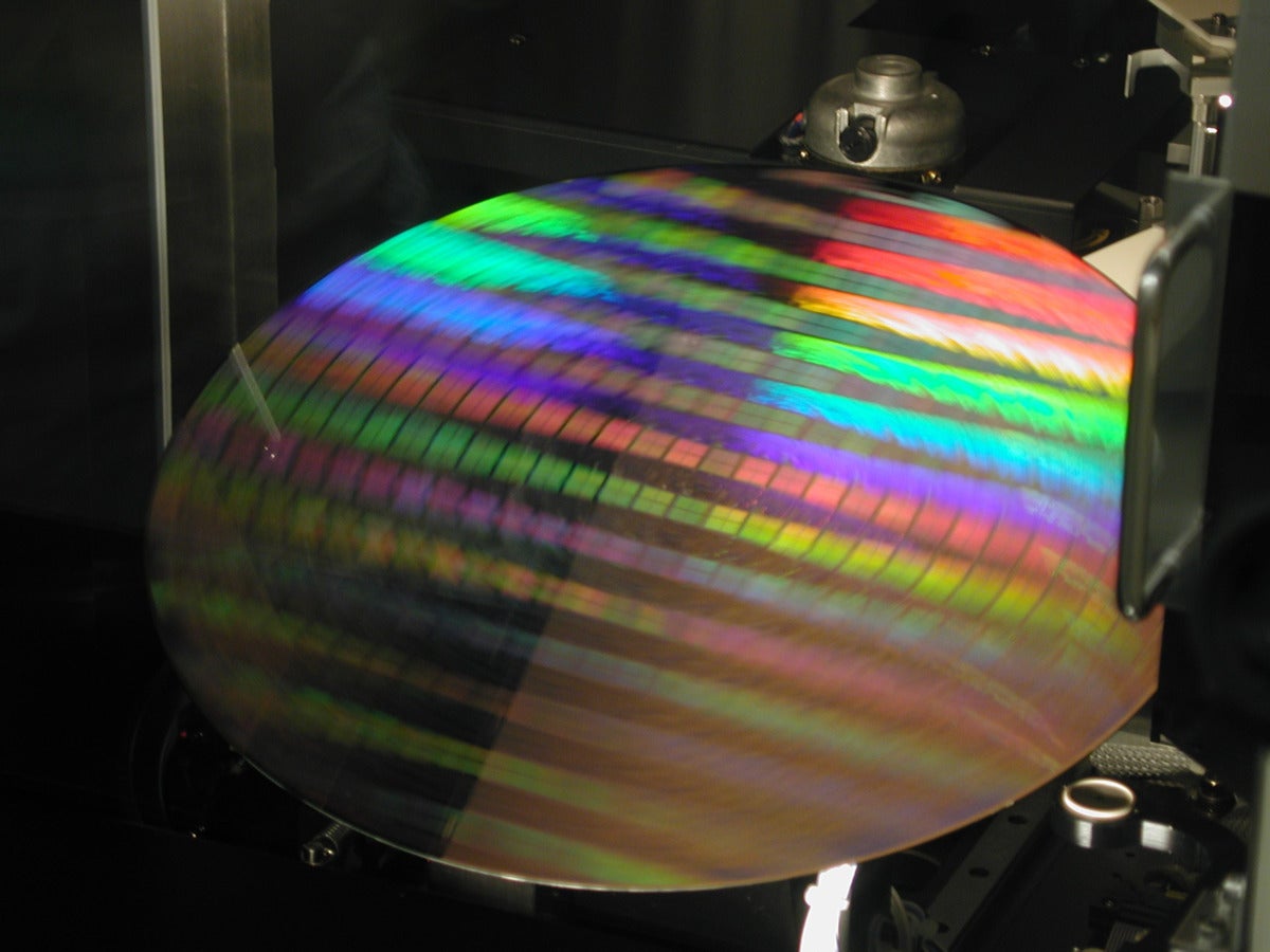
IBM leapfrogs everyone with its 2nm chips

As TSMC charges to 5nm transistor designs and Intel struggles for 7nm, IBM has topped them all with the world’s first 2-nanometer node chip.
OK, it won’t come to market for four years, according to IBM, and they might not be the first name that comes to mind when you think of processor design, but they are the quiet power in the semiconductor world.
As far as commercial chips go, IBM makes two: the Power series for its Power line of Unix and Linux servers, and zArchitecture that is used in the z Series of mainframes. But IBM has its IBM Joint Development Alliance which is partnered with just about every semiconductor vendor out there—Intel, AMD, Nvidia, TSMC, Samsung, you name it.
IBM claims that the technology can fit “50 billion transistors onto a chip the size of a fingernail.” No word on whether that’s a pinky fingernail or a thumb. The company also claims its 2nm development will improve performance by 45% at the same power, or 75% less energy use at the same performance, compared to a 7nm processor.
So what does this mean? According to IBM it means:
- Quadrupling cell phone battery life, requiring users to charge their devices only every four days.
- Slashing the carbon footprint of data centers, which account for 1% of global energy use. Changing all of their servers to 2nm-based processors could potentially reduce that number significantly.
- Drastically speeding up laptop functions, ranging from quicker processing in applications, to assisting in language translation, to faster internet access.
- Contributing to faster object detection and reaction time in autonomous vehicles like self-driving cars.
For you nerds out there, IBM achieved this shrink through a new manufacturing process called Gate-All-Around, which stacks the transistors in 3D. It’s an advance on FinFET 3D stacking. (Quite frankly, I have a hard time figuring it out. Here is a deep dive if you are interested and can get your head around it.)
IBM isn’t high profile in semiconductor research, but its presence is formidable. IBM is the king of intellectual property, earning more patents every year than the rest of the industry, and it is happy to make a deal with just about anyone.
IBM has one of the world’s leading research centers on future semiconductor technology in Albany, New York, where it works closely with Rensselaer Polytechnic Institute, a school up there with MIT when it comes to STEM programs.
So expect everyone from Intel to TSMC to be at 2nm in about five years, at which point transistors will be about the size of an atom.
Copyright © 2021 IDG Communications, Inc.

